Scalable Wafer Level Production of Consumables Made of Non-CMOS Compatible Materials on Glass, Challenges and Opportunities Utilizing a Foundry Concept
Alexios Tzannis, Business Development Manager, IMT Masken und Teilungen AG
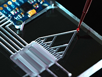
For many microfluidic applications glass remains the material of choice. Glass is inert to most chemicals, has unsurpassed and well defined optical properties and good temperature and pressure stability. Glass components, however, have a reputation for being too expensive for high volume applications. In this presentation we show that this paradigma is wrong, if manufacturing technology developed for semiconductors is applied. The manufacturing of these components requires the whole portfolio of wafer-level packaging (WLP) processes, such as generation of (sub-)µm structures, through glass Vias (TGVs), temporary and/or permanent bonding. Life Science and Lab-on-a-Chip (LOAC) applications often require the integration of structured electrodes or waveguides. Therefore patterning of non-CMOS compatible materials as well as the compatibility of the processes to the constraints biological matter is needed. Whilst the mass production of sub µm patterns is well established in the semiconductor industry, semiconductor fabs are limited to using CMOS compatible materials. IMT of Switzerland has implemented a fully automated manufacturing line that allows cost effective mass manufacturing of consumables in substrate materials like borosilicate or fused silica wafers. The applied processes offer a high degree of freedom in the design of the consumable. In this presentation we discuss the challenges and solutions of implementing WLP processes for LOAC products.
|
|


 Add to Calendar ▼2016-09-26 00:00:002016-09-28 00:00:00Europe/LondonLab-on-a-Chip and Microfluidics: Companies, Technologies and CommercializationSELECTBIOenquiries@selectbiosciences.com